Well, I’ve been thinking a lot lately about single board computers. There’s a big market out there. Since the Raspberry Pi, there’s been a real explosion available to the small-end of town, the individual. Prior to this, development boards were mostly in the 4-figures sort of price range.
So we’re now rather spoiled for choice. I have a Raspberry Pi. There’s also the BeagleBone Black, Banana Pi, and several others. One gripe I have with the Raspberry Pi is the complete absence of any kind of analogue input. There’s an analogue line out, you can interface some USB audio devices (although I hear two is problematic), or you can get an I2S module.
There’s a GPU in there that’s capable of some DSP work and a CLKOUT pin that can generate a wide range of frequencies. That sounds like the beginnings of a decent SDR, however one glitch, while I can use the CLKOUT pin to drive a mixer and the GPIOs to do band selection, there’s nothing that will take that analogue signal and sample it.
If I want something wider than audio frequencies (and even a 192kHz audio CODEC is not guaranteed above ~20kHz) I have to interface to SPI, and the pickings are somewhat slim. Then I read this article on a DIY single board computer.
That got me thinking about whether I could do my own. At work we use the Technologic Systems TS-7670 single-board computers, and as nice as those machines are, they’re a little slow and RAM-limited. Something that could work as a credible replacement there too would be nice, key needs there being RS-485, Ethernet and a 85 degree temperature rating.
Form factor is a consideration here, and I figured something modular, using either header pins or edge connectors would work. That would make the module easily embeddable in hobby projects.
Since all the really nice SoCs are BGA packages, I figured I’d first need to know how easy I could work with them. We’ve got a stack of old motherboards sitting in a cupboard that I figured I could raid for BGAs to play with, just to see first-hand how fine the pins were. A crazy thought came to me: maybe for prototyping, I could do it dead-bug style?
Key thing here being able to solder directly to a ball securely, then route the wire to its destination. I may need to glue it to a bit of grounded foil to keep the capacitance in check. So, the first step I figured, would be to try removing some components from the boards I had laying around to see this first-hand.
In amongst the boards I came across was one old 386 motherboard that I initially mistook for a 286 minus the CPU. The empty (PLCC) socket is for an 80387 math co-processor. The board was in the cupboard for a good reason, corrosion from the CMOS battery had pretty much destroyed key traces on one corner of the board.
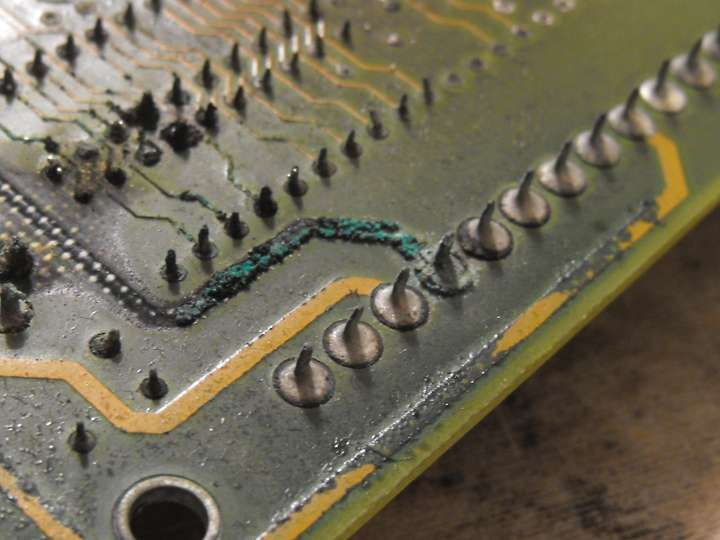
Corrosion on a motherboard caused by a CMOS battery
I decided to take to it with the heat gun first. The above picture was taken post-heatgun, but you can see just how bad the corrosion was. The ISA slots were okay, and so where a stack of other useful IC sockets, ICs, passive components, etc.
With the heat gun at full blast, I’d just wave it over an area of interest until the board started to de-laminate, then with needle-nose pliers, pull the socket or component from the board. Sometimes the component simply dropped out.
At one point I heard a loud “plop”. Looking under the board, one of the larger surface-mounted chips had fallen off. That gave me an idea, could the 386 chip be de-soldered? I aimed the heat-gun directly at the area underneath. A few seconds later and it too hit the deck.
All in all, it was a successful haul.

Parts off the 386 motherboard
I also took apart an 8-bit ISA joystick card. It had some nice looking logic chips that I figured could be re-purposed. The real star though was the CPU itself:
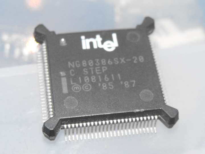
Intel NG80306SX-20
The question comes up, what does one do with a crusty old 386 that’s nearly as old as I am? A quick search turned up this scanned copy of the Intel 80386SX datasheet. The chip has a 16-bit bus with 23 bits worth of address lines (bit 0 is assumed to be zero). It requires a clock that is double the chip’s operating frequency (there’s an internal divide-by-two). This particular chip runs internally at 20MHz. Nothing jumped out as being scary. Could I use this as a practice run for making an ARM computer module?
A dig around dug up some more parts:
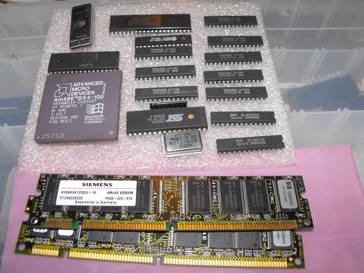
More parts
In this pile we have…
I also have some SIMMs laying around, but the SDRAM modules look easier to handle since the controllers on board synchronise with what would otherwise be the front-side bus. The datasheet does not give a minimum clock (although clearly this is not DC; DRAM does need to be refreshed) and mentions a clock frequency of 33MHz when set to run at a CAS latency of 1. It just so happens that I have a 33MHz oscillator. There’s a couple of nits in this plan though:
- the SDRAM modules a 3.3V, the CPU is 5V: no problem, there are level conversion chips out there.
- the SDRAM modules are 64-bits wide. We’ll have to buffer the output to eight 8-bit registers. Writes do a read-modify-write cycle, and we use a 2-in-4 decoder to select the CE pin on two of the registers from address bits 1 and 2 from the CPU.
- Each SDRAM module holds 32MB. We have a 23-bit address bus, which with 16-bit words gives us a total address space of 16MB. Solution: the old 8-bit computers of yesteryear used bank-switching to address more RAM/ROM than they had address lines for, we can interface an 8-bit register at I/O address 0x0000 (easily decoded with a stack of Schottky diodes and a NOT gate) which can hold the remaining address bits mapping the memory to the lower 8MB of physical memory. We then hijack the 386’s MMU to map the 8MB chunks and use the page faults to switch memory banks. (If we put the SRAM and ROM up in the top 1MB, this gives us ~7MB of memory-mapped I/O to play with.)
So, not show stoppers. There’s an example circuit showing interfacing an ATMega8515 to a single SDRAM chip for driving a VGA interface, and some example code, with comments in German. Unfortunately you’d learn more German in an episode of Hogan’s Heroes than what I know, but I can sort-of figure out the sequence used to read and write from/to the SDRAM chip. Nothing looks scary there either. This SDRAM tutorial seems to be a goldmine.
Thus, it looks like I’ve got enough bits to have a crack at it. I can run the 386 from that 33MHz brick; which will give me a chip running at 16.5MHz. Somewhere I’ve got the 40MHz brick laying around from the motherboard (I liberated that some time ago), but that can wait.
A first step would be to try interfacing the 386 chip to an AVR, and feed it instructions one step at a time, check that it’s still alive. Then, the next steps should become clear.


 Seems Vicis has had a similar idea, their


Recent Comments